

Step-By-Step Guide to PCB Manufacturing Process
PCBs work as a backbone for all significant electronics, from cellphones to microwaves. These extraordinary inventions are present in almost all computational electronics, no matter how simple or complicated they might be. The PCB market itself is worth $12.86 billion in the US.
What is a PCB?
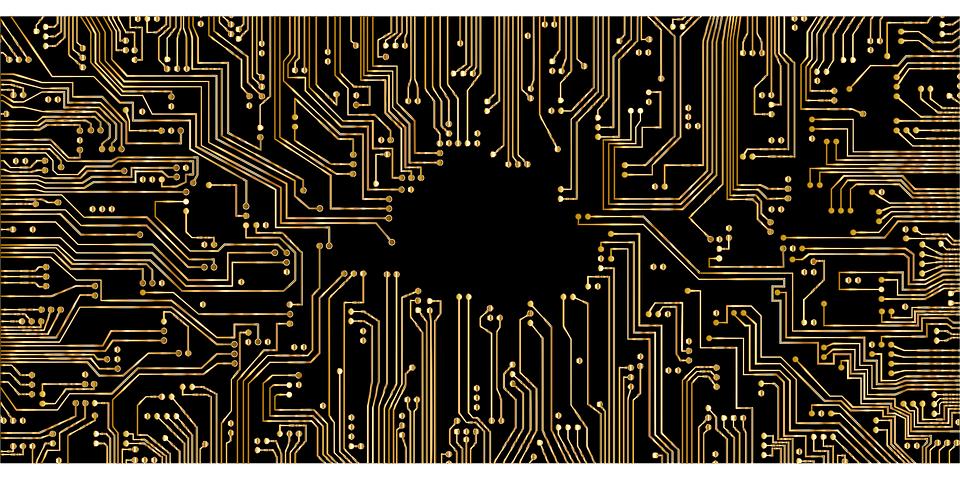
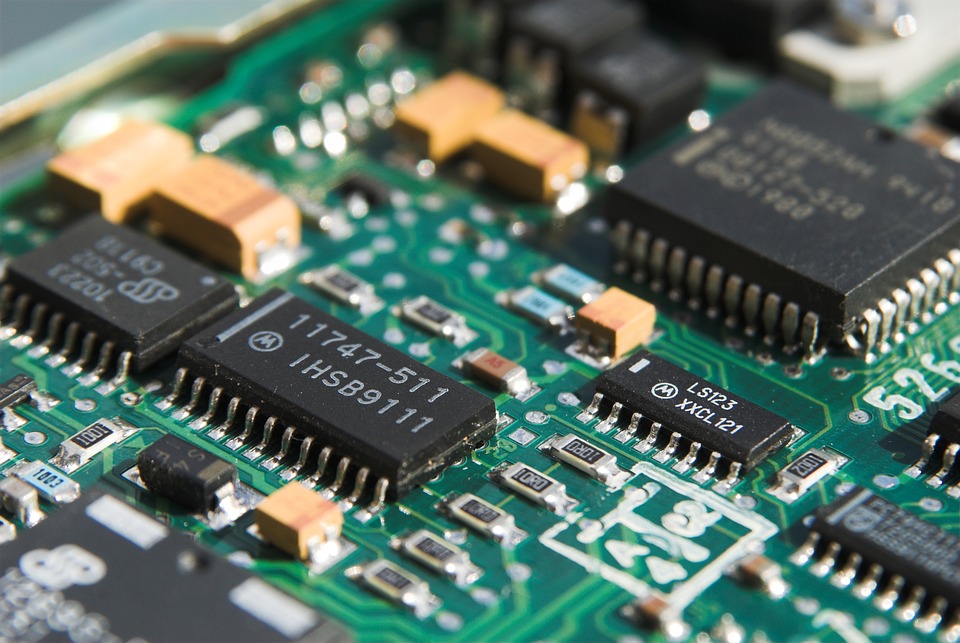
A Printed Circuit Board (PCB) is responsible for connecting the components in a device electronically to bring it to life. This miraculous invention ties all electronic components together by being the primary source of guidance for electricity. All electronic components are attached to the PCB using a metal wire that conducts electricity.
How are PCBs Made?
Now that we understand what PCBs are, let’s discuss how a PCB is manufactured.
Step 1: Design and Output
Most PCBs are made by applying a layer of copper on the entire surface of the substrate material on one side or both to create a blank PCB covered in copper. Based on the design of the pattern, the unwanted copper is removed using a subtractive method.
Step 2: The Journey from File to Film
To remove the copper from the circuit board’s substrate, a process called photoengraving is used that is masked with chemical etching to “subtract” the cupper. This photoengraving process is done using a photoplotter and sometimes a laser printer.
Step 3: Stick Together
All PCBs are made using multiple layers of the PCB, which are stuck together to create one uniform PCB. These layers are called multilayers, and are made of thin trace or etched boards bonded together through lamination.
Step 4: Time for the Drill
For the PCB to work flawlessly, each layer of the PCB should connect with another to pass the electricity. This is done by drilling small holes in the PCB called “VIAS.” These holes are precision placed and must be done using an automated drilling machine to be as accurate as possible.
Step 5: Copper Conductors
In order to connect the electronic components with the PCB, copper wires are used as conductors. But copper can mount to PCB itself, which is why a medium is used to help adhere it. Previously it used to be tin, but now nickel or gold is used for increased solderability.
Step 6: Silk Screen
Every company wants its logo and other instructions embedded on the PCB to distinguish it from other brands. The silk-screening process is used to make this happen.
Step 7: Let’s Put it To the Test
The last step is assembling everything and putting the PCB board to the test. This is where you detect all the possible errors that might be there or wiring issues that need correction.
Need the best of the best PCB assembly service for your product? Hop onto Find An EMS today. We are one of the most satisfactory OEM and EMS provider partnering services in the US who can help you connect with the right service provider for the job.
Get in touch with us today to learn more.